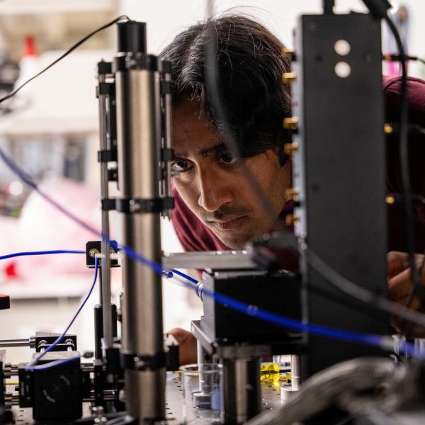
By taking advantage of the unique properties of materials at very small scales, researchers are poised to explore fundamental questions about electronic structures and quantum phenomena.
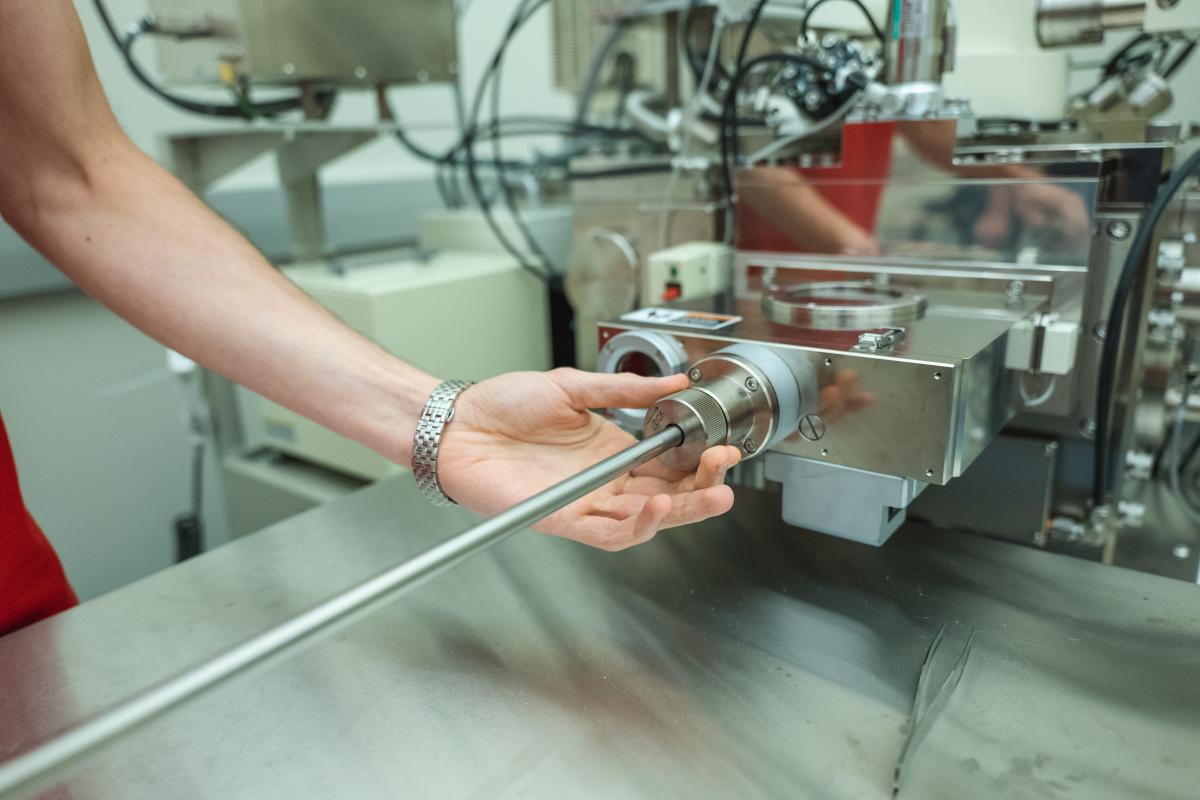
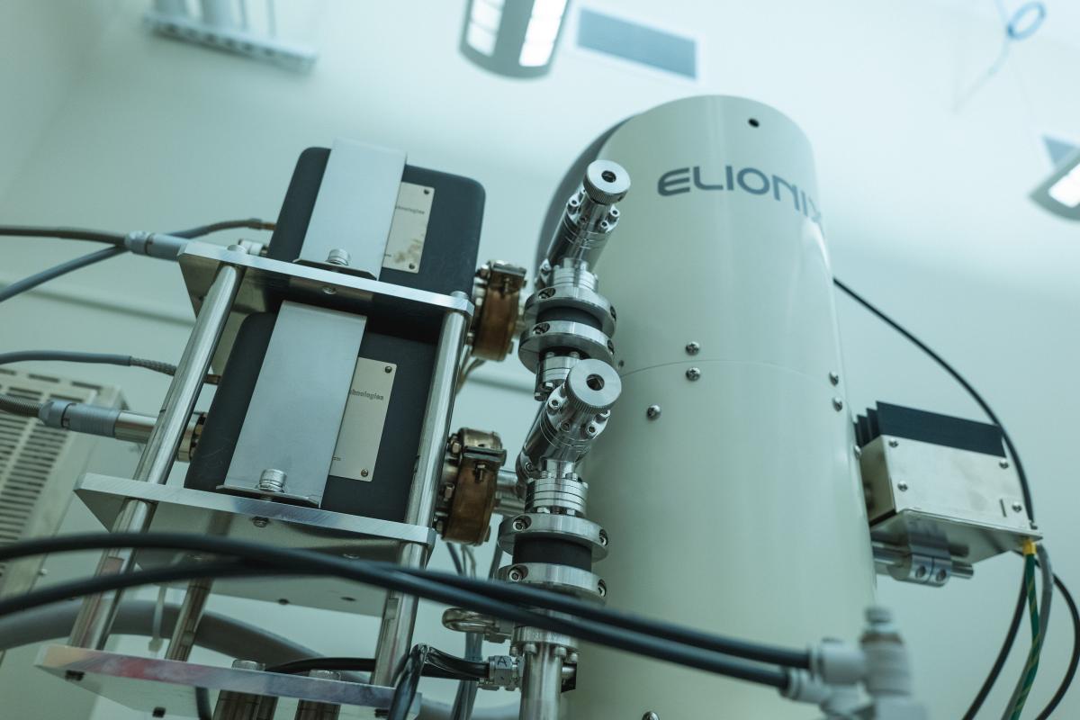
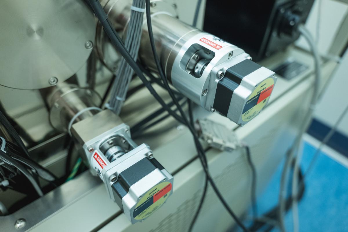
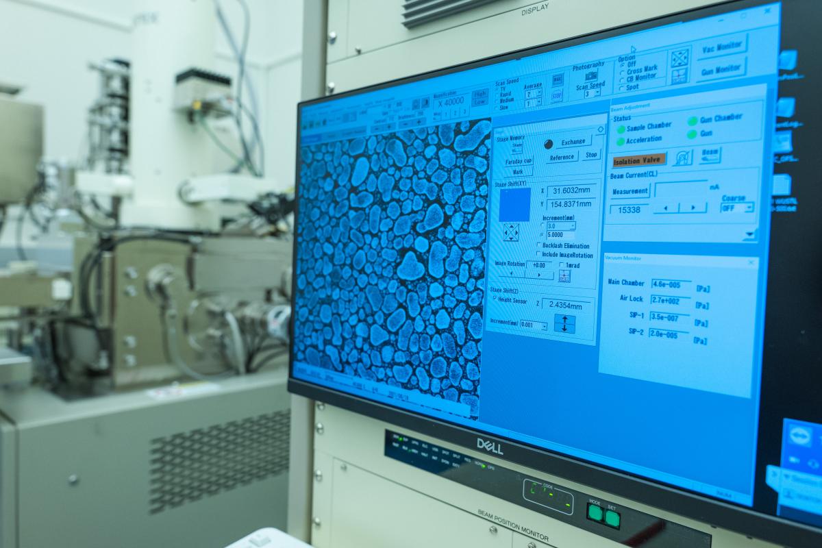
A strand of human hair is roughly 100,000 nanometers wide. Last month, Washington University installed a new instrument capable of creating nano-scale patterns with features 10,000 times smaller – just 10 nanometers wide. The new electron beam lithography system, the Elionix ELS-S50EX, is housed in the Institute of Materials Science & Engineering (IMSE).
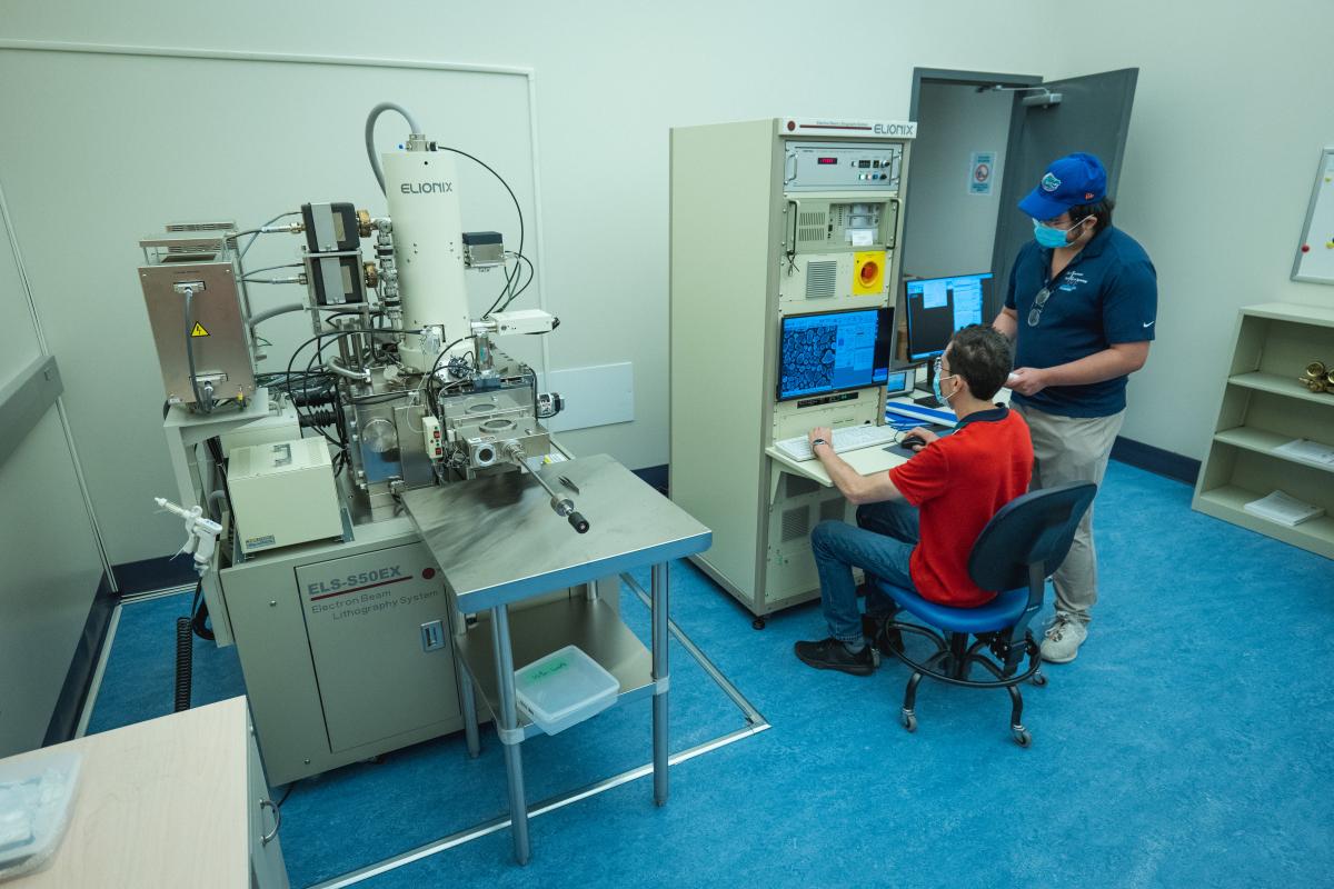
Scientists across Arts & Sciences and the university will use the new facility to conduct research where micron- and nanometer-sized circuits or patterns in semiconductors and metals are employed to explore and control electronic and optical properties of materials. Applications include producing circuit elements for quantum information science, creating photonic circuits based on light, controlling the nano-scale flow of heat, and more. By taking advantage of the unique properties of materials at very small scales, researchers in Arts & Sciences are poised to explore fundamental questions about electronic structures and quantum phenomena.
The $1 million electron beam lithography system was purchased by Kater Murch, professor of physics in Arts & Sciences, with support from the IMSE; Erik Henriksen, associate director of IMSE and associate professor of physics in Arts & Sciences; and Mark Lawrence, assistant professor in the Department of Electrical and Systems Engineering in the McKelvey School of Engineering. The facility will be available for shared use by all IMSE members. In Arts & Sciences, Henriksen anticipates that most users will come from the departments of Physics and Chemistry.
Beyond Murch, Henriksen, and Lawrence, another regular user is likely to be Bryce Sadtler, assistant professor of chemistry, who investigates light-induced chemical transformations in inorganic nanostructures. In addition to their work in quantum mechanics and emergent quantum phenomena, Murch and Henriksen also collaborate with James Buckley, professor of physics, on the Axion Dark Matter Experiment (ADMX).
“ADMX is a really exciting project for us and a great example of how this new facility will be used,” Henriksen said. “We’re in charge of the ‘cold electronics’ for ADMX and are developing new quantum device technologies that will make extensive use of the new lithography system. We’re fabricating things like specialized parametric amplifiers, which are used to amplify specific signals when making quantum-limited measurements.”
This facility is Henriksen’s first major installation since taking on the role of associate director of IMSE July 1. As associate director, Henriksen brings his extensive cleanroom experience to the task of overseeing IMSE’s facilities. He also works with IMSE director Katharine Flores to strategize future research directions and pursue new equipment and funding to best serve the institute’s approximately 50 member groups.